Verification evidence for the SEC module
The SEC module was evaluated at four levels: individual blocks, connected subsystems, the full APB-facing module, and FPGA bring-up with an external flash device. Several security-relevant invariants are also encoded as SystemVerilog assertions in the RTL, so they are checked throughout simulation runs.
Summary: 13 self-checking testbenches, 400+ automatic checks, a
cycle-oriented model of the Winbond flash, five named security assertions inside
main_fsm.sv, and a 24-page stress test passing on FPGA hardware
(11/11). Beyond correctness, the module was instrumented for
on-board profiling, exercised through a browser live-demo GUI, and is
going through its first ASIC synthesis bring-up. Numbers below are from the
latest local Vivado XSim 2025.1 and Icarus Verilog runs.
Four levels of testing
The verification flow is organized bottom-up. Individual modules are checked first, then the interfaces between modules, then the full SEC module at the APB boundary, and finally the FPGA implementation. This makes many failures local to the level where they are introduced.
One block at a time
Each module is exercised in isolation against a hand-written reference: FIFOs, the ASCON core, the BCH coder, the PUF, the HDA, the counter, the Quad-SPI master, the trace ring, and the PCU. These tests cover local corner cases with short simulation times.
Chains of blocks
Real blocks wired together exactly as in the design — status_ctrl+FIFO,
fuzzy extractor+ASCON, the full main_fsm with ASCON, counter and
Quad-SPI master. These tests focus on handshakes and data transfer between
modules.
The whole module
The complete SEC subsystem driven from a behavioral APB master — the same view the RISC-V firmware has. Boot, enrollment, encryption, decryption, sector isolation, and the debug-key path are tested end to end through RTL.
FPGA hardware
Synthesised to an FPGA and driven by actual RISC-V firmware against a physical W25Q64JV flash over the PMOD connector. This level also exercises board wiring, I/O timing, and signal-integrity effects.
Self-checking testbench results
Each testbench prints an explicit verdict by comparing against a reference model
or expected sequence and counting PASS/FAIL checks.
These are the latest local results.
| Level | Testbench | Result | Coverage focus |
|---|---|---|---|
| system | tb_tum_ss_system | 66/66 | Full flow at the APB boundary: QE-init, enroll (PUF→BCH→HDA→W), encrypt a page, decrypt & authenticate, second-page isolation, debug key + AD flag |
| integration | tb_sec_main_fsm_flow | 54/54 | Main-FSM regression: enroll + counter reservation, write/read roundtrip (58 words), reservation-ceiling crossing, power-cycle restore, fresh-nonce check, debug-key path |
| integration | tb_sec_cmd_arbitration | 18/18 | The one-request pending slot: a second request during busy is rejected (sticky req_dropped), the in-flight one survives, later requests resume |
| integration | tb_status_ctrl | 83/83 | APB front-end: the 58-word write sequence, every sequence-error case, RX protocol, the debug-key registers & key_source |
| integration | tb_fe_subsystem | 15/15 | Fuzzy-extractor chain under real i.i.d. PUF noise: enroll, reset, reconstruct from a different PUF read — the recovered key equals the enrolled key |
| integration | tb_fe_subsystem_sv_uvm | 31/31 | Fuzzy extractor, UVM-style: enroll, reconstruct, re-enroll, back-to-back stress, and the hash-corruption security property — all with 0 assertion failures |
| unit | tb_spi_master_quad | 19/19 | Quad-SPI master against the flash model: QE-init, helper-data writes, encrypted writes, the address-guard violation, a quad read-back |
| unit | tb_qspi_trace | 21/21 | The read-only command-trace ring: entry/status/count views, wrap behaviour, erase/program/read tallies |
| unit | tb_pcu | 39/39 | Performance-counter unit: windowed metrics, the internal drop/stall derivation, the FIFO high-water/average and BCH-error mirrors, clean elaboration with the block switched on and off |
| unit | tb_sram_macro | 7/7 | Port contract of the real foundry SRAM-PUF macro (ASIC path): active-low chip enable, read/write polarity, one-cycle read latency, bit-write mask |
| unit | tb_fifo_core | 80/80 | The FIFO at the heart of every data path: fill/drain, almost-full thresholds, flush, and the overflow/underflow assertions |
| unit | tb_ascon_control · tb_ascon_core | pass | ASCON-AEAD128 encrypt/decrypt round-trip and ASCON-Hash256 — the cryptographic engine itself |
| fpga | sec_multipage_test | 11/11 | 24 pages across two sectors on hardware — in-order & reverse read, cross-sector isolation, nonce +1 per encryption, no dropped requests |
Several older bring-up testbenches (the 4-word-protocol encrypt chains) are kept in the tree for historical reference and are explicitly marked deprecated — the rows above are the authoritative regression set.
Security-relevant RTL assertions
In addition to the testbenches, key invariants are encoded in the design as
SystemVerilog assertions (`ifndef SYNTHESIS, simulation only). They
are evaluated on every relevant cycle and stop the simulation if the invariant is
violated.
Plaintext only after authentication
mc_rx_push_o |-> (ascon_auth_valid && ascon_auth)
No decrypted word may reach the RX FIFO before the authentication tag has been verified. If a record is modified, tag verification fails and the plaintext is not released.
Application access excludes provisioning
app op |-> app_sector_r >= FIRST_APP_SECTOR
Every erase, program and read that belongs to an application record must target the application area — never the helper-data / hash / counter region. The assertion checks that the Main FSM does not request such an access.
No push into a full FIFO
qspi_tx_push_o |-> !qspi_tx_full_i
Back-pressure is honoured: the Main FSM never enqueues a flash command when the command FIFO is full.
ASCON commanded only when ready
ascon_cmd_valid_r |-> $past(ascon_cmd_ready)
A crypto command is issued only after ASCON has signalled it can accept one, preserving the ready/valid handshake.
One request at a time
ready_o |-> !(app_wr_start_i && app_rd_start_i)
A read and a write can never both launch in the same cycle; this checks the single-outstanding request arbitration.
FIFO bounds
p_no_overflow · p_no_underflow · p_count_range
In every FIFO: no push when full, no pop when empty, and the element count always stays within bounds.
Role of assertions: a testbench checks selected scenarios, while an assertion checks an invariant across all scenarios that reach the relevant signal condition. The fuzzy-extractor UVM suite runs its six groups with 0 assertion failures.
Behavioral flash model
w25q64jv_model.sv is a behavioral model of the Winbond W25Q64JV used
by the Quad-SPI testbenches. It implements the opcodes, Mode-0 timing, and status
registers used by the design.
- Status Register 1 (
BUSY,WEL) and Register 2 (QE) modelled bit-for-bit. - The five commands the design uses:
WREN,RDSR1,WRSR2, Quad Page Program and Fast Read Quad Output. - After every page program,
BUSYis set so the master's poll loop is actually exercised, then cleared. - A memory array so written bytes can be read back and compared.
Model implementation note: an early version split the flash logic across
four event-driven blocks (on SCLK edges, on CS edges, and on the clock). Simulator
event scheduling caused the read-status decoder to fire one clock late, so the
master waited indefinitely for BUSY to clear. The model now runs from
a single clocked process and decodes each command on the edge that receives it.
On-chip observability
The SEC module exposes internal status through APB-readable registers. The same observability points are used in simulation and on FPGA hardware:
Every FSM state, live
The Main-FSM state (0x008), ASCON's FSM (0x014) and the
counter FSM are all readable over the bus. Firmware and testbenches alike can observe the
machine progress through boot → encrypt → decrypt in real time.
See the state map →
QSPI command trace
A 16-entry ring (0x040) records every flash command — type and address —
plus erase/program/read tallies. After an encrypt you can confirm "1 erase, 64 programs"
and the exact order. How the flash talks →
Performance counters
An optional PCU (0x150) counts dropped requests, accepted ops, run cycles
and flash-FIFO stalls — raw numbers for measuring throughput on hardware, switched off
entirely when area is tight. PCU reference →
FPGA bring-up
Passing simulation is necessary, not sufficient. The design was synthesised to an FPGA and driven by real RISC-V firmware against a physical W25Q64JV over the PMOD connector — the first environment that includes board wiring, I/O timing, and the physical flash device.
- Firmware test programs drive the full sequence over APB and read the status, error and observability registers back over UART.
- The multi-page stress test (
sec_multipage_test) writes and reads 24 records across two sectors and checks in-order & reverse reads, cross-sector isolation, a fresh nonce per encryption and no dropped requests — 11/11 on hardware. - The first SoC synthesis surfaced a name collision between an internal
counterinstance and a library cell; the instance was renamed and the relevant simulations were re-run.
Hardware debug example
FPGA bring-up exposed a quad-SPI read issue that was not visible in the purely digital flash model. Helper-data read-back returned a small number of incorrect words, with different counts across bitstreams.
| Step | What we saw | What it ruled out |
|---|---|---|
| 1 · symptom | Each error was a consistent 1-nibble (4-bit) slip, not a random bit error. The lost nibble almost always had DQ3=1 & DQ0=1, indicating data dependence. | Suggested a structural issue on the quad lines rather than random noise. |
| 2 · repeated read | Reading one address three times returned different values. | Pointed to the read path rather than persistent flash contents. |
| 3 · independent dump | An ESP32 read the flash contents back correctly. | Confirmed the flash contents and the write path. |
| 4 · single-line check | Reading the same bytes over one data line (Fast Read 0x0B) was always clean. | Localized the issue to the quad DQ read path. |
Root cause. During a quad read, the eight dummy cycles are a bus turnaround: the
master must release the DQ lines so the flash can start driving them. The dummy
state was running in the driving branch and held all four DQ lines
low until the data phase. At the dummy→data handover, the master's low
drive conflicted with the flash driving DQ3/DQ0 high,
matching the observed data dependence.
Fix: switch the dummy state into receive mode so the master tri-states the
DQ lines during the turnaround. Single-line reads and quad writes are unchanged.
The digital simulator cannot reproduce analog bus contention, but it confirmed no
regression; the hardware [S] self-test confirmed the fix on FPGA.
Performance & silicon cost
Two questions beyond "is it correct": how fast does an operation run, and how much hardware does the module cost. The first is measured on the FPGA prototype; the second comes from a first ASIC synthesis of the SEC subsystem.
Operation timing (FPGA prototype — measurement pending)
A dedicated firmware test (sec_perf_test, on the live-demo branch)
brackets each operation with Ibex's free-running mcycle counter, so
the cycle delta is the exact wall-clock cost (cycles ÷ fclk = seconds).
The measured window is kept UART-silent — the result line is printed only after
the timer is stopped — so the 9600-baud log cannot inflate the figure. Covered
operations: one-time boot enrollment, page write with and without the
4 KB sector erase, authenticated read, and an N-page burst; the optional
PCU supplies dropped-request and flash-stall counts for the same run.
No board numbers yet. The instrumentation and the GUI-side plotting are implemented, but the measurement run on the FPGA board is still pending, so no cycle figures are published here. What the hardware tests have already shown qualitatively: the 4 KB flash erase dominates a write into a fresh sector, and the multipage stress test sustained 24 page operations with 0 dropped requests.
Silicon cost (ASIC synthesis bring-up)
The SEC subsystem (tum_ss) is being taken through its first
standard-cell synthesis with Synopsys tooling against a GF 22 nm
library, within the subsystem's 350 × 350 µm² floorplan budget.
The first runs were used to clean up RTL constructs that simulation and FPGA
synthesis tolerate but the ASIC elaborator rejects — an oversized
function-local lookup table and a cross-generate reference in the
BCH chain (details).
In progress — no numbers yet. The elaboration blockers are fixed in the RTL, but a complete synthesis run (with the SRAM-PUF macro library linked) has not finished yet. Cell counts, area, and timing will be published here once a full run exists; until then the only committed figure is the floorplan budget above.
Live-demo GUI
For demos and bring-up, the FPGA tests are also driven from a small browser
GUI. It builds, loads and runs a chosen fpga/sw test at the press
of a button, streams the UART log live, and — the centrepiece — paints the
external flash as a colour-coded sector/page map as the module writes, reads
and authenticates records in real time.
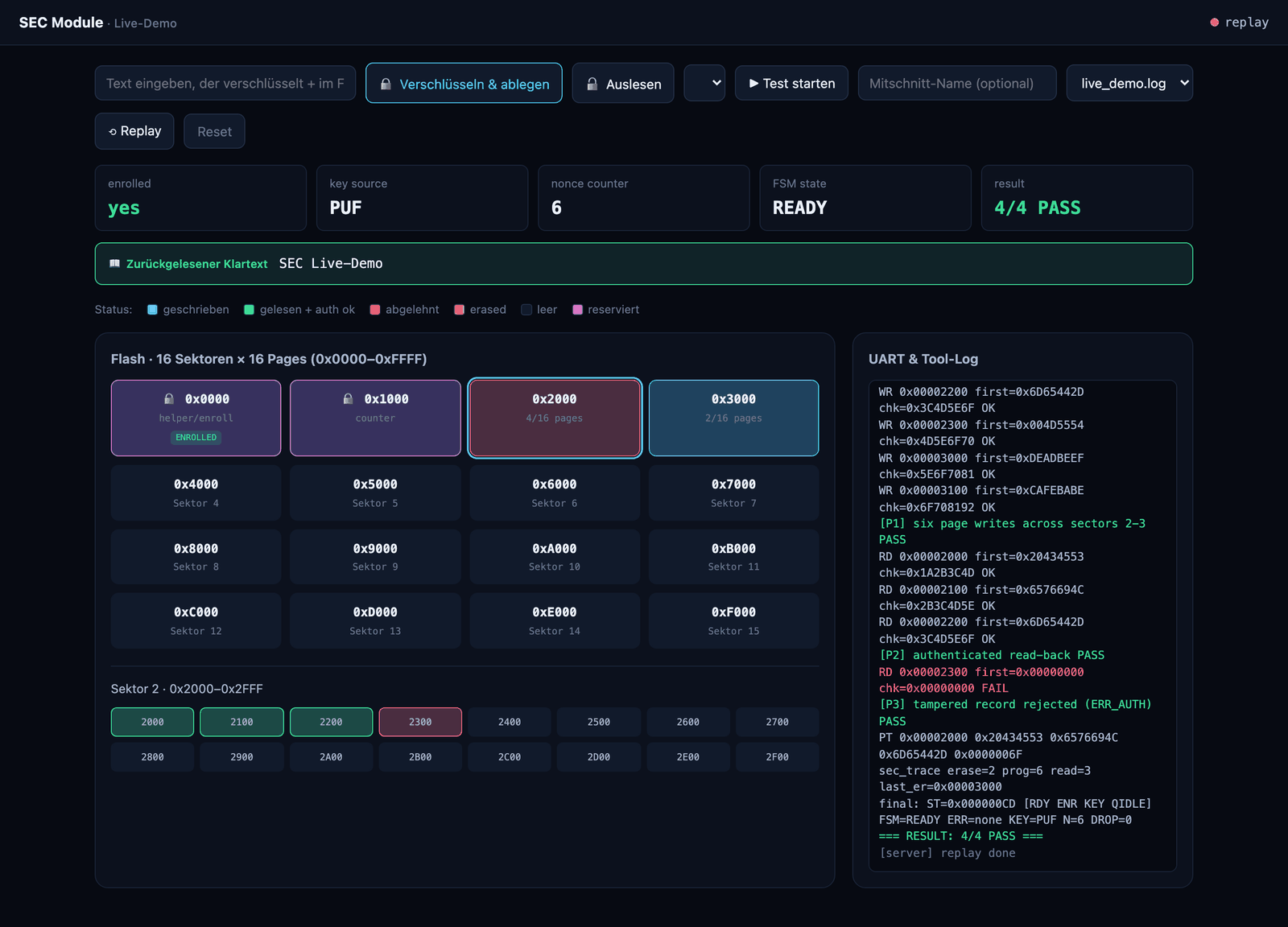
ENROLLED) and sector 1 (counter) are reserved.
Page colours: ■ written · ■ read + auth OK · ■ rejected (ERR_AUTH) · ■ erased · ■ empty · ■ reserved (helper / counter)
Dependency-light by design
A pure Python-stdlib backend (http.server + server-sent events)
and a vanilla HTML/CSS/JS frontend reusing this site's theme. The only optional
package is pyserial, and only for the live board link.
Encrypt your own text
Type a message; the GUI packs it into 58-word pages, generates the C firmware, builds, loads over JTAG and runs it — then reads the record back and shows where in flash it landed.
Replay mode
Any captured *.log replays through the same parser pipeline, so
the whole visualisation runs from a file — for slides, video, or a demo without
hardware.
The GUI lives on the demo/live-gui branch. Its optional
raw-flash-byte view depends on a read-only RTL path that is
`ifdef-gated and never compiled into the ASIC build.
Toolchain
| Tool | Role |
|---|---|
| Vivado XSim 2025.1 | Primary RTL simulator for the SystemVerilog regression set and synthesis to FPGA |
| Synopsys Fusion / Design Compiler | ASIC synthesis bring-up of the tum_ss subsystem against a GF 22 nm library (elaboration clean-up done, first complete run pending) — see Performance & silicon cost |
| Standard-cell library | GF 22 nm FDX target technology, with the SRAM-PUF as the single hard macro |
| Icarus Verilog | Fast local smoke checks for unit testbenches (e.g. the QSPI trace ring) |
| GTKWave / Vivado waves | Waveform inspection when a check needs a closer look |
| PyUVM + cocotb | Python UVM framework for APB-level register and stimulus tests |
| RISC-V GCC firmware | Bare-metal C drivers running the module on the FPGA, reporting over UART |
| OpenOCD + GDB | Loads the bitstream firmware and runs the bring-up tests over JTAG; also drives the live-demo GUI runner |
House rules. Reset is async, active-low throughout. Addresses and sizes come from one
source of truth — sec_pkg.sv — never hard-coded in a test. After any change that
touches the RTL, the relevant testbenches are re-run and the x/y PASS result is
logged before the work is considered done.